

SEGA Rally 2 Driver Board Force Feedback GAL Reverse Engineering
SEGA Rally 2 Championship was probably the best rally racing game for arcades in 1998 but a lot of gamers agree that SEGA Rally 2 is still nowadays the best rally cabinet arcade. SEGA Rally 2 was (is) famous for the realism of the Force FeedBack (FFB) steering wheel.
The core of the FFB is the Driver Board where the FFB commands are received from the main computer (SEGA Model 3), processed and transferred to the power module in order to move the steering wheel.
The Driver Board is an electronic board which mounts a lot of components. One of this component is a Lattice GAL16V8, a programmable IC. In this article I’m going to describe how I have made a reverse engineering of the GAL16V8 to obtain the internal logic.

SEGA Rally 2 championship twin arcade cabinet
The FFB is realized in the SEGA Rally 2 cabinet using 4 main components:
- The SEGA Model 3 main computer which sends, through a serial bus, the FFB commands to the Driver Board. The serial commands have already been studied by few users. See these links for more info about the type of commands and how to drive the Driver Board externally:
http://superusr.free.fr/model3.htm
https://github.com/njz3/vJoyIOFeederWithFFB
https://github.com/njz3/vJoyIOFeederWithFFB/blob/master/DRIVEBOARD.md - The Driver Board receives the FFB commands from the SEGA Model 3 and the feedback from the Motor Board. The Driver Board processes the commands received according to the feedback and drives the Motor Board;
- The Motor Board is driven by the Driver Board and contains the electronic components to drive the DC Motor mounted below the steering wheel.
- The DC Motor is mechanically connected to the steering wheel.
In the image below, a list of SEGA games with different types of FFB.
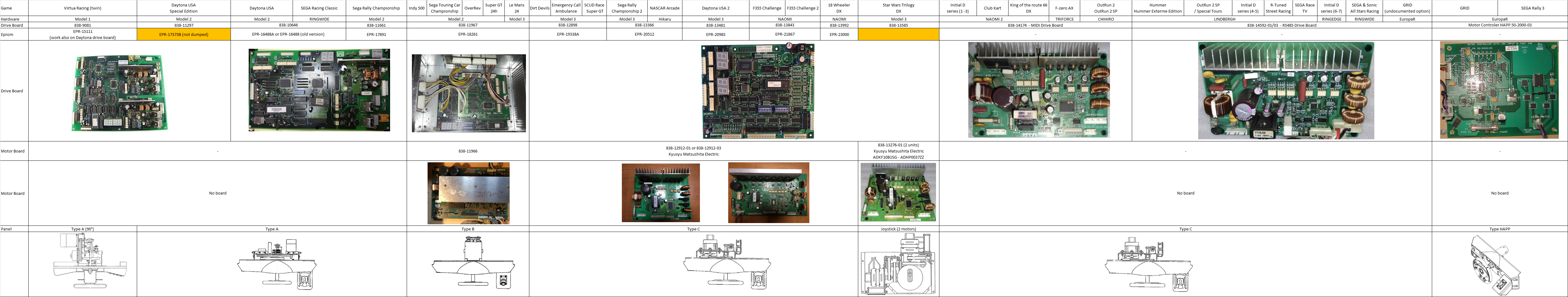
List of Board/EEPROM (Thanks to BigPanik and njz3 for the great work!!!)
The Driver Board is composed by a lot of electronic components mostly produced by Toshiba (which are very hard to find nowadays).
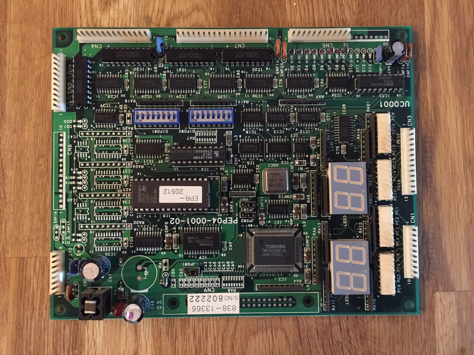
SEGA Rally 2 Driver Board
A list of the main components of the Driver Board is reported here:
- IC3 – Microcontroller (Toshiba TMPZ84C015BF-10);
- IC9 – SRAM (Toshiba TC55257DFI-85L);
- IC8 – EEPROM (ST M27C512-15FI);
- IC4 – GAL (Lattice GAL16V8D-15LP);
- OSC1 – 16MHz Oscillator;
- IC7 – IC Reset Circuit;
- IC33 – ADC (OKI MSM6253);
- LED2/LED3 – 7 segment display.
The Driver Board is used in multiple SEGA cabinet games (see “List of Board/EEPROM” figure). The hardware is exactly the same but the code in the instruction memory contained in the EEPROM changes, therefore how FFB is processed changes as well. The EEPROM of a lot of games have already been dumped and the .bin can be found with Google (inside MAME ROMS), so the replacement of the EEPROM in the Driver Board is quite easy to achieve.
The big issue while repairing the Driver Board is GAL16V8D which contains a programmable logic. The logic inside the GAL16V8D is unknown, so replacing this IC was impossible (until now).
So, I decided to make a reverse engineering of the logic inside the GAL16V8D and to post the combinational logic and the JEDEC file to be programmed inside a new Lattice GAL16V8D for free, as a gift for SEGA cabinet repairer.
The reverse engineering process starts analyzing the Driver Board schematic to find which are the input and the output pins of the GAL16V8D. The schematic is not very simple so I decided to skip this description and post the Input/Output of the GAL16V8D:
|
1 2 3 4 5 6 7 8 9 10 11 12 13 14 15 16 17 18 19 20 21 |
- INPUT- pin 1 (I/CLK) pin 2 (I) pin 3 (I) pin 4 (I) pin 5 (I) pin 6 (I) pin 7 (I) pin 8 (I) pin 9 (I) pin 11 (I/OE) - OUTPUT - pin 12 (I/O/Q) pin 13 (I/O/Q) pin 14 (I/O/Q) pin 15 (I/O/Q) pin 16 (I/O/Q) pin 17 (I/O/Q) pin 18 (I/O/Q) pin 19 (I/O/Q) |
While analyzing the schematic it is clear that the logic inside the GAL is pure combinational without state machine or clock process. This makes the reverse engineering process simpler: to understand the logic inside the GAL is possible to drive all signals combinations in Inputs and to observe all the Outputs. To do this operation (applicable to every GAL not only for SEGA Rally 2) I have used an Arduino MEGA to drive every Inputs pin of the GAL16V8D and to observe every Outputs pin. Every Output is pull-upped to assure that the GAL really drove the Outputs.

Arduino MEGA with GAL16V8D
The code I have written for Arduino MEGA is the following:
|
1 2 3 4 5 6 7 8 9 10 11 12 13 14 15 16 17 18 19 20 21 22 23 24 25 26 27 28 29 30 31 32 33 34 35 36 37 38 39 40 41 42 43 44 45 46 47 48 49 50 51 52 53 54 55 56 57 58 59 60 61 62 63 64 65 66 67 68 69 70 71 72 73 74 75 76 77 78 79 80 81 82 83 84 85 86 87 88 89 90 91 92 93 94 95 96 97 98 99 100 101 102 103 104 105 106 107 108 109 110 111 112 113 114 115 116 117 118 119 120 121 122 123 124 125 126 127 128 129 130 131 132 133 134 135 136 137 138 139 140 141 142 143 144 145 146 147 148 149 150 151 152 153 154 155 156 157 158 159 160 161 162 163 164 165 166 167 168 169 170 171 172 173 174 175 176 177 178 179 180 181 182 183 184 185 186 187 188 189 190 191 192 193 194 195 196 197 198 199 200 201 202 203 204 205 206 207 208 209 210 211 212 213 214 215 216 217 218 219 220 221 |
---------------------------------------------------------------- -- -- Project: SEGA RALLY 2 Driver Board GAL16V8 Replacement -- Company: AC Engineer -- -- Software name: SR2DriverBoardRevEng -- Description: Arduino MEGA software to make -- Lattice GAL16V8D (IC4) Reverse Engineering -- for SEGA Rally 2 cabinet Driver Board -- -- File Name: SR2DriverBoardRevEng.ini -- -- Author: Alessio Carpini -- Revision: 1.1 -- Date: 04-08-2023 -- ---------------------------------------------------------------- // Input Pin /* Struct Index <--> GAL16V8 <--> ARDUINO MEGA - INPUT- - OUTPUT - [0] pin 1 (I/CLK): pin 37 [1] pin 2 (I): pin 36 [2] pin 3 (I): pin 35 [3] pin 4 (I): pin 34 [4] pin 5 (I): pin 33 [5] pin 6 (I): pin 32 [6] pin 7 (I): pin 31 [7] pin 8 (I): pin 30 [8] pin 9 (I): pin 49 [9] pin 11 (I//OE): pin 48 - OUTPUT - - INPUT - [10] pin 12 (I/O/Q): pin 22 [11] pin 13 (I/O/Q): pin 23 [12] pin 14 (I/O/Q): pin 24 [13] pin 15 (I/O/Q): pin 25 [14] pin 16 (I/O/Q): pin 26 [15] pin 17 (I/O/Q): pin 27 [16] pin 18 (I/O/Q): pin 28 [17] pin 19 (I/O/Q): pin 29 */ struct definePinAssociated { uint8_t GAL16V8_pin; char GAL16V8_name[5]; uint8_t MEGA_pin; } ; definePinAssociated inOutStruct[18]; void setup() { // Input/Output/Name Assignments // 0 inOutStruct[0].GAL16V8_pin = 1; inOutStruct[0].MEGA_pin = 37; strcpy(inOutStruct[0].GAL16V8_name, "in1"); // 1 inOutStruct[1].GAL16V8_pin = 2; inOutStruct[1].MEGA_pin = 36; strcpy(inOutStruct[1].GAL16V8_name, "in2"); // 2 inOutStruct[2].GAL16V8_pin = 3; inOutStruct[2].MEGA_pin = 35; strcpy(inOutStruct[2].GAL16V8_name, "in3"); // 3 inOutStruct[3].GAL16V8_pin = 4; inOutStruct[3].MEGA_pin = 34; strcpy(inOutStruct[3].GAL16V8_name, "in4"); //4 inOutStruct[4].GAL16V8_pin = 5; inOutStruct[4].MEGA_pin = 33; strcpy(inOutStruct[4].GAL16V8_name, "in5"); // 5 inOutStruct[5].GAL16V8_pin = 6; inOutStruct[5].MEGA_pin = 32; strcpy(inOutStruct[5].GAL16V8_name, "in6"); // 6 inOutStruct[6].GAL16V8_pin = 7; inOutStruct[6].MEGA_pin = 31; strcpy(inOutStruct[6].GAL16V8_name, "in7"); // 7 inOutStruct[7].GAL16V8_pin = 8; inOutStruct[7].MEGA_pin = 30; strcpy(inOutStruct[7].GAL16V8_name, "in8"); //8 inOutStruct[8].GAL16V8_pin = 9; inOutStruct[8].MEGA_pin = 49; strcpy(inOutStruct[8].GAL16V8_name, "in9"); // 9 inOutStruct[9].GAL16V8_pin = 11; inOutStruct[9].MEGA_pin = 48; strcpy(inOutStruct[9].GAL16V8_name, "in11"); // 10 inOutStruct[10].GAL16V8_pin = 12; inOutStruct[10].MEGA_pin = 22; strcpy(inOutStruct[10].GAL16V8_name, "ou12"); // 11 inOutStruct[11].GAL16V8_pin = 13; inOutStruct[11].MEGA_pin = 23; strcpy(inOutStruct[11].GAL16V8_name, "ou13"); // 12 inOutStruct[12].GAL16V8_pin = 14; inOutStruct[12].MEGA_pin = 24; strcpy(inOutStruct[12].GAL16V8_name, "ou14"); // 13 inOutStruct[13].GAL16V8_pin = 15; inOutStruct[13].MEGA_pin = 25; strcpy(inOutStruct[13].GAL16V8_name, "ou15"); // 14 inOutStruct[14].GAL16V8_pin = 16; inOutStruct[14].MEGA_pin = 26; strcpy(inOutStruct[14].GAL16V8_name, "ou16"); // 15 inOutStruct[15].GAL16V8_pin = 17; inOutStruct[15].MEGA_pin = 27; strcpy(inOutStruct[15].GAL16V8_name, "ou17"); // 16 inOutStruct[16].GAL16V8_pin = 18; inOutStruct[16].MEGA_pin = 28; strcpy(inOutStruct[16].GAL16V8_name, "ou18"); // 17 inOutStruct[17].GAL16V8_pin = 19; inOutStruct[17].MEGA_pin = 29; strcpy(inOutStruct[17].GAL16V8_name, "ou19"); // pinMode for INPUT definition according to defined struct int i=0; for(i=0; i<10; i++) { pinMode(inOutStruct[i].MEGA_pin, OUTPUT); } // pinMode for OUTPUT definition according to defined struct for(i=10; i<18; i++) { pinMode(inOutStruct[i].MEGA_pin, INPUT); } // initialize serial communication: Serial.begin(115200); } void loop() { int16_t i = 0; uint16_t j = 0; uint16_t pinSelect = 0; // Print Header for(i=9; i>=0; i--) { Serial.print(inOutStruct[i].GAL16V8_name); Serial.print(", "); } for(i=10; i<18; i++) { Serial.print(inOutStruct[i].GAL16V8_name); if(i < 17) { Serial.print(", "); } else { Serial.println(""); } } // Setting the Output for(j=0; j < 1024; j++) { pinSelect = 1024; for(i=9; i>=0; i--) { if(i > 0) { pinSelect = pinSelect >> 1; digitalWrite(inOutStruct[i].MEGA_pin, (j & pinSelect) >> i); Serial.print((j & pinSelect) >> i); Serial.print(", "); } else { digitalWrite(inOutStruct[0].MEGA_pin, (j & 0x0001)); Serial.print(j & 0x0001); Serial.print(", "); } } // In order to stabilize GAL output delay(20); // ---- ---- // // Input Reading for(i=10; i<18; i++) { Serial.print(digitalRead(inOutStruct[i].MEGA_pin)); if(i < 17) { Serial.print(", "); } else { Serial.println(""); } } } Serial.println("END"); while(1); } |
After the reset, Arduino MEGA starts to drive the Inputs and reads the Outputs. The result of every combination is printed in the Serial console where it is possible to make a Copy and Paste in a .csv. The CSV can be imported in an Excel sheet to better analyze the combination. Below, a screenshot of the Excel file with the first part of the Inputs/Outputs combination.

EXCEL GAL Combinational Logic (only first part)
After analyzing the Inputs/Outputs, the following combinational logic can be found. The logic is described in VHDL.
|
1 2 3 4 5 6 7 8 9 10 11 12 13 14 15 16 17 18 19 20 21 22 23 24 25 26 27 28 29 30 31 32 33 34 35 36 37 38 39 40 41 42 43 44 45 46 47 48 49 50 51 52 53 54 55 56 57 58 59 60 61 62 63 64 65 66 67 68 69 70 71 72 73 74 75 76 77 78 79 80 81 82 83 84 85 86 87 88 89 90 91 92 93 94 95 |
---------------------------------------------------------------- -- -- Project: SEGA RALLY 2 Driver Board GAL16V8 Replacement -- Company: AC Engineer -- -- Module name: e_SR2DriverBoard -- Description: Replacement in VHDL for SEGA RALLY 2 -- Driver Board GAL16V8D IC4 -- PEP04-0001-02 (838-12898) (838-13481) -- -- File Name: e_SR2DriverBoard.vhd -- -- Author: Alessio Carpini -- Revision: 1.1 -- Date: 04-08-2023 -- ---------------------------------------------------------------- LIBRARY IEEE; USE IEEE.STD_LOGIC_1164.ALL; USE IEEE.NUMERIC_STD.ALL; ENTITY e_SR2DriverBoard IS PORT ( -- Input PIN l_SR2DriverBoardInPin1_i : IN STD_LOGIC; l_SR2DriverBoardInPin2_i : IN STD_LOGIC; l_SR2DriverBoardInPin3_i : IN STD_LOGIC; l_SR2DriverBoardInPin4_i : IN STD_LOGIC; l_SR2DriverBoardInPin5_i : IN STD_LOGIC; l_SR2DriverBoardInPin6_i : IN STD_LOGIC; l_SR2DriverBoardInPin7_i : IN STD_LOGIC; l_SR2DriverBoardInPin8_i : IN STD_LOGIC; l_SR2DriverBoardInPin9_i : IN STD_LOGIC; l_SR2DriverBoardInPin11_i : IN STD_LOGIC; -- Output PIN l_SR2DriverBoardInPin12_o : OUT STD_LOGIC; l_SR2DriverBoardInPin13_o : OUT STD_LOGIC; l_SR2DriverBoardInPin14_o : OUT STD_LOGIC; l_SR2DriverBoardInPin15_o : OUT STD_LOGIC; l_SR2DriverBoardInPin16_o : OUT STD_LOGIC; l_SR2DriverBoardInPin17_o : OUT STD_LOGIC; l_SR2DriverBoardInPin18_o : OUT STD_LOGIC; l_SR2DriverBoardInPin19_o : OUT STD_LOGIC ); --The syntax of attribute LOC --attribute LOC : string; --attribute LOC of [SigName] : signal is "[pin#]"; attribute LOC : string; attribute LOC of l_SR2DriverBoardInPin1_i : signal is "1"; attribute LOC of l_SR2DriverBoardInPin2_i : signal is "2"; attribute LOC of l_SR2DriverBoardInPin3_i : signal is "3"; attribute LOC of l_SR2DriverBoardInPin4_i : signal is "4"; attribute LOC of l_SR2DriverBoardInPin5_i : signal is "5"; attribute LOC of l_SR2DriverBoardInPin6_i : signal is "6"; attribute LOC of l_SR2DriverBoardInPin7_i : signal is "7"; attribute LOC of l_SR2DriverBoardInPin8_i : signal is "8"; attribute LOC of l_SR2DriverBoardInPin9_i : signal is "9"; attribute LOC of l_SR2DriverBoardInPin11_i : signal is "11"; attribute LOC of l_SR2DriverBoardInPin12_o : signal is "12"; attribute LOC of l_SR2DriverBoardInPin13_o : signal is "13"; attribute LOC of l_SR2DriverBoardInPin14_o : signal is "14"; attribute LOC of l_SR2DriverBoardInPin15_o : signal is "15"; attribute LOC of l_SR2DriverBoardInPin16_o : signal is "16"; attribute LOC of l_SR2DriverBoardInPin17_o : signal is "17"; attribute LOC of l_SR2DriverBoardInPin18_o : signal is "18"; attribute LOC of l_SR2DriverBoardInPin19_o : signal is "19"; END e_SR2DriverBoard; ARCHITECTURE a_SR2DriverBoard OF e_SR2DriverBoard IS SIGNAL l_toggleOutput_s : STD_LOGIC; SIGNAL l_outputEnable_s : STD_LOGIC; BEGIN l_toggleOutput_s <= l_SR2DriverBoardInPin8_i AND l_SR2DriverBoardInPin9_i AND l_SR2DriverBoardInPin11_i; l_outputEnable_s <= NOT(l_SR2DriverBoardInPin5_i) OR l_SR2DriverBoardInPin6_i OR l_SR2DriverBoardInPin7_i; l_SR2DriverBoardInPin12_o <= l_toggleOutput_s; l_SR2DriverBoardInPin13_o <= NOT(l_toggleOutput_s); l_SR2DriverBoardInPin14_o <= l_outputEnable_s OR l_SR2DriverBoardInPin4_i OR l_SR2DriverBoardInPin3_i OR l_SR2DriverBoardInPin2_i; l_SR2DriverBoardInPin15_o <= l_outputEnable_s OR l_SR2DriverBoardInPin3_i OR NOT(l_SR2DriverBoardInPin2_i); l_SR2DriverBoardInPin16_o <= l_outputEnable_s OR l_SR2DriverBoardInPin4_i OR NOT(l_SR2DriverBoardInPin3_i); l_SR2DriverBoardInPin17_o <= l_outputEnable_s OR NOT(l_SR2DriverBoardInPin4_i) OR NOT(l_SR2DriverBoardInPin3_i); l_SR2DriverBoardInPin18_o <= l_outputEnable_s OR NOT(l_SR2DriverBoardInPin4_i) OR l_SR2DriverBoardInPin3_i OR NOT(l_SR2DriverBoardInPin2_i); l_SR2DriverBoardInPin19_o <= NOT(l_SR2DriverBoardInPin5_i XOR l_SR2DriverBoardInPin6_i XOR l_SR2DriverBoardInPin7_i) OR l_SR2DriverBoardInPin1_i; END ARCHITECTURE a_SR2DriverBoard; |
In this article I described how to synthetize a VHDL for the GAL16V8D using the Lattice ispLEVER software. I will not repeat the procedure where but if you are interested you can read the article. Note: The article is written in Italian but you can use an online translator (Like Google Translate) to understand the procedure.
As a gift I decided to release, for free, the JEDEC file (.jed) ready to be programmed in a brand new GAL16V8D (see bottom page).
If you like this article and I helped you with a (big) problem, please donate me e coffee, I’ll be very happy!!!
Bye bye, have a nice day and happy holidays!!!


